 EN
EN  AR
AR FR
FR DE
DE JA
JA PT
PT CN
CNTellurium Zinc cadmium detector for design of low noise readout circuit
Tellurium Zinc Cadmium semiconductor materials at room temperature have such advantages as high resistivity, small temperature coefficient, easy to be combined with front-end electronics, high sensitivity, etc.In order to meet the requirements of high resolution and integration in PET electronic imaging system, a low-noise front-end readout circuit based on tellurium zinc cadmium semiconductor materials was designed.
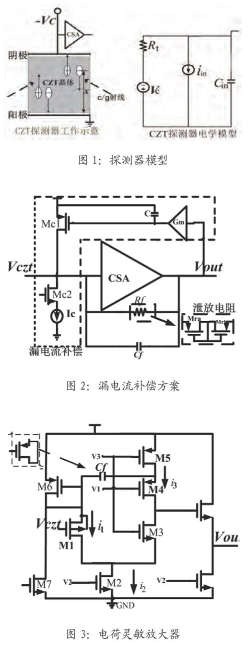
1. Detector model
As shown in the left figure of figure 1, the working diagram of CZT detector shows that when the ray enters the tellurium zinc cadmium detector, it interacts with the CZT crystal to produce electron-hole pairs. When a high bias VC is applied to the cathode, the electron-hole pairs generated by ionization in the crystal drift towards the two plates respectively. Thus, the charge in the depletion layer region of the detector moves the distance of dx to the collection electrode in dt time, and the inductive charge of dQin is generated on the collection electrode. This charge is collected by the charge sensitive amplifier, so the instantaneous current is generated on the cathode electrode plate. Therefore, the CZT detector can be equivalent to the electrical model shown in the right figure in figure 1, and the electrode capacitance and wired distributed capacitance of the detector can be equivalent to the input capacitance cin. The current pulse iin generated on the probe plate; Id leakage current.
2.1 Leakage current compensation circuit
As shown in figure 2, the leakage current influences the stability of circuit noise and output baseline through Rf of feedback resistance, and adopts the parallel structure of leakage current compensation circuit and self-biased virtual resistance: Mc1 and Mc2 working in the sub-threshold area realize leakage current compensation, and Ic is the compensation current of 2nA.Mra and Mrb in series the feedback resistance Rf and its resistance to G Ω magnitude, the resistance to avoid two consecutive period of superposition of electric charge.
2.2 Charge sensitive amplifier reduces noise realization
To increase the gain of the circuit can also reduces the output equivalent noise charge. For this reason, the charge sensitive amplifier in this paper adopts a foldable co-source co-gate structure, as shown in figure 3. M1, M2, M3, M4, M5 constitute a single-end folding amplifier, whose noise is half of the differential structure. The noise of the circuit mainly comes from the white noise and 1/f noise of MOS tube. Figure 3 circuit noise model is as follows: i2≈i1 and i3/i1 are achieved through appropriate design.
Through leakage current compensation circuit, MOS virtual resistance and circuit low-noise design and shaping, at room temperature, when the input capacitance is 5pF, the equivalent noise charge is lower than 132e.When the leakage current changes from 0nA to 2nA, the output baseline of the circuit is kept at 590mV and the deviation of each process Angle is less than 30nV, which can meet the requirements of subsequent signal processing.
Product recommendation : Tellurium
Changsha SANTECH provides Tellurium Metal Ingot, Tellurium Metal Granule, Tellurium Metal Powder, Tellurium Dioxide Powder, etc. Please email us if you are interested in our products. Thank you!